
Silicon Ingot Ductile chamfering
Silicon Ingot Ductile polish-grinding & chamfering MPS 3-134 High precision surface and chamfer grinding machine to finish mono- and multi-crystalline and UMG silicon bricks for solar wafer. Detailed Specs Silicon Ingot Ductile polish-grinding & chamfering MPS 3-134 High precision surface and chamfer grinding machine to finish mono- and multi-crystalline and UMG silicon bricks for solar wafer. – Ductile polish-grinding method – 50% Si wafer breakage reduction – Prepared for in-line-system (robot-loading) – Twin-spindle ® grinding concept for rough and fine / finish grinding of the surfaces – Second grinding spindle for simultaneously chamfering the edges of the brick – Grinding of the surfaces and the edges in the same clamping position (no rechucking / handling in between) – Automatic handling (loading, unloading, turning) of the brick – Automatic grinding progress with integrated measuringWAFER BREAKAGE REDUCTION – Ductile polish grinding for solar bricks helps to reduce wafer breakage significantly
...more
Polysilicon Filament Cutter
LDSS 1/2/4, Specially developed for filament production Logomatic Diamond Seed Saw To produce poly silicon seeds, a seed arc is needed in the reactor (Siemens). The arc is manufactured of 2 slim rods and one top bridge connection. The thin rods height is between 1,800 – 3,000mm with a squared dimensions of usually 8x8mm (12×12 and 10x10mm are also known) The new technology by using DIAMOND WIRE as slicing tool it can cut in a cross over wire with 4 rods of 150 mm OD simultaneously in one operation.
...more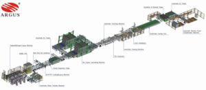
panel turnkey line
Fully Automatic turnkey line for module production – Stringer & Tabber – Laminator – Auto Framing Machine – LASER Scriber – EVA Cutting Machine – EL Tester – Cell Sorter and Tester Argus Solar is the market leader in the solar energy industry, Argus Solar designs and develops manufacturing lines and equipment for photovoltaic panels. The company provides solutions ranging from a 5 MW PV module production line to a 300 MW line, The principle of the PV Turnkey Project of Wuhan Sunic Photoelectricity Equipment Manufacture Co., LTD has always been to take care of every detail in our clients’ production and reduce labor dependency and land usage so as to create competency for our clients in terms of cost while improving production efficiency and capability. The assembly line consist of: Tabber&Stringer, Auto Lay-up Machine, EL Tester( before/after laminating), Conveyor Units, Auto Laminating Machine, Auto Trimming Machine, Auto Framing Machine, Auto Curing Line, IV Module Tester, Auto Module Sorting Machine and other solar module inspection equipment. This solution with high standard equipment and high automation is in the leading edge of the industry. Nevertheless, the designed assembly line is beautiful and neat with high cost efficiency which allows convenient manipulation and maintenance.
...more
Multi Crystalline Silicon Ingot Squaring
LDQS 690 / 840 / 1100 For multicrystalline silicon ingots with the sizes from 690 to 1100 mm² (height max. 500 mm) – Water based coolant instead of slurry – QUICK, SIMPLE loading and unloading – Automatic cutting process Advantages compared to conventional slurry wire saw: – Higher cutting speed (fixed abrasive) – Less spare and wear parts management – Less investment expense – Less energy consumption – Less footprint – Less operating personnel
...more
Multi Crystalline Silicon cropping
Multi-Crystalline Silicon Ingot Top & bottom grinding LBG 690 / 840 / 1100 Developed for multi-crystalline silicon ingots: By removing the contaminated top surface it is possible, when reclaiming the cropped parts, to raise wafer yield of the next crystallized ingot. Detailed Specs Advantages: – High throughput with low costs – Significant material waste reduction – Less risk of wire breakage for squaring – Flat surfaces for further processing – Save up to 3% costs of wafer manufacturing – Mechanical clamping – Automatic grinding process
...more
Mono Crystalline Silicon Squarer
Mono-Crystalline Silicon Ingot Squarer LDQS 16 / 25 / 36 For squaring of monocrystalline silicon ingots Detailed Specs Water based coolant instead of slurry: – QUICK, SIMPLE loading and unloading – Simple ingot clamping – Automatic cutting process Advantages compared to conventional slurry wire saw: – Higher cutting speed (fixed abrasive) – Less spare and wear parts management – Less investment expense – Less energy consumption – Less footprint – Less operating personnel
...more
Metal Chemical Vapor Deposition system
Valence Process Equipment offers both production and research-sized MOCVD reactor systems for Group III-Nitride and InGaAl-AsP material systems. We can provide a high degree of customization to suit your specific process requirements. Valence Process Equipment patented, 500-series platform features a non clogging, temperature-controlled showerhead gas injector, and our high symmetry, minimized-volume, non-recirculating pro led reactor, enabling production-level capacities with pilot-level gas and MO usage. Along with high speed wafer carrier rotation, rapid heating capability to 1200C, and high-velocity, uniform- fluid gaps providing efficient heat removal and uniform wall temperatures, the 500-series provides state-of-the-art epitaxial materials properties and uniformities at unbeatable efficiencies. CAPACITY SPECIFICATIONS: – 250- series capacity – 10x2in, 5x3in, 3x4in, 1x6in, 1x8in – 500-series capacity – 72x2in, 20x4in, 7x6in, 4x8in FACILITY SERVICES: – 208 and 380 VAC, 3- Phase Power – Purified N2, H2, and NH3 Gases – Cooling Water Recirculation Loop – Cabinet and Exhaust Ventilation MATERIAL SPECIFICATIONS: – GaN, InGAN, AIGaN, AIN – 2 in., 3 in., 6 in., 8 in. Substrates – Sapphire, Silicon, Silicon Carbide.
...more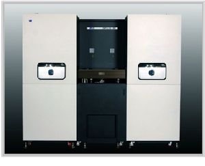
Ion Implantation Reactors
Kingstone’s IonSolar – Ion implantation forms high quality PN junctions that improve solar cell conversion efficiency and also significantly simplifies the fabrication processes of various high efficiency solar cells. Kingstone has designed a new ion implanter specifically tailored to the PV industry IonSolar™. On both the wafer handling and beam line modules, IonSolar™ introduced patented breakthroughs: a””curtain-like”” ion beam that can implant multiple wafers simultaneously, and a wafer handling platform that allows continuous wafer implanting without waiting for wafer exchanges. IonSolar™ makes possible field retrofittable upgrades of existing solar cell production lines in order to achieve higher efficiency cell manufacturing. IonSolar™ Features – High productivity production throughput of 1800 wafers / hour, matching the pacing of existing production lines – Small footprint 22m2, fitting into space requirements of existing production lines – Low CoO 40% reduction compared to similar systems, allowing for ROI in less one year
...more
Ingot Lifetime scanning machine
The LL 156/300 is designed to evaluate material quality quickly and economically. This handy machine helps to guarantee a steady quality of wafers Detailed Specs – Mapping of carrier lifetime, photoconductivity, resistivity – Non-contact, non-destructive electrical semiconductor characterisation – Two dimensional ingot mapping system for solar grade multi silicon – Measurement time: 2 minutes for two surfaces simultaneously – One ingot four sides with handling: 5 – 6 min – Resolution 1 mm
...more
Ingot Infrared inspection machine
The LBA 300 3D is designed and built especially to inspect multicrystalline silicon bricks for PV wafer production. Detailed Specs – Reliable detection of microcracks and SiC inclusions – Reduction of wire breakage by wafering – Increase of wafer yield – Quick cycle time – Loading manually or automatically (in-line) – 3D brick model – Analyzing of ingot crystallization result
...more
Groove Grinding Machine
The LGG is designed to grind and regroove the wire guides from slurry wafering saws or diamond wire saws to any pitch size. Detailed Specs The machine is designed to regrind OD and regroove the wire guides from e. g. Logomatic (Diamond Multi Wire Saw), Linton, HCT, Meyer+Burger, Themis, NTC-Japan, Toyo and Takatory and all other slurry or diamond wire saws, which need refurbishing of wire guide rolls. This machine can grind OD sizes from 2 – 13 inches (50-350 mm), with high precision pitch for a length from 100 – 1000 mm.
...more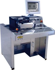
Bond Alignment Systems
EVG offers high precision, fully integrated and highly automated wafer Bond Aligner systems for bonding application such as anodic, silicon fusion, thermo-compression and eutectic bonding. The alignment and bonding process separation results in higher flexibility and universal application of the wafer bonding equipment. The EVG bond alignment systems offer highest precision, flexibility, ease of use and modular upgrade capability and have been qualified in numerous high throughput production environments. The precision of EVG bond aligners accommodates most demanding alignment processes in MEMS production and in emerging fields like 3D integration applications. A maximum level of automation and process integration is achieved by the GEMINI Automated Production Wafer Bonding System. Wafer-to-wafer alignment and wafer bonding processes up to 200 mm (300 mm) for volume manufacturing are all performed in one fully automated platform. Device manufacturers benefit from increased production output, a high integration level and a big choice of process variations like anodic, silicon fusion, thermo-compression and eutectic bonding. Ultra clean handling of wafers throughout the bonding process assures high-yield and void-free bonds. All essential steps, from cleaning and alignment to pre-bonding and IR-inspection are combined in one high volume production system. EVG850 is the only production bonding system built to operate in high throughput, high-yield environments and guarantees void-free SOI wafers up to 300 mm.
...more
Atomic layer deposition system
Atomic layer deposition (ALD) provides a unique method for depositing defect free ultrathin films on surfaces. This technique uses sequential surface reactions to coat substrates with high conformality and precise thickness control at the atomic scale. Atomic layer deposition (ALD) provides a unique method for depositing defect free ultrathin films on surfaces. This technique uses sequential surface reactions to coat substrates with high conformality and precise thickness control at the atomic scale.The ALD(Atomic Layer Deposition) process consists of sequential introduction of desired precursor vapors with hydroxyl groups, each of which forms about one atomic layer per pulse. Key challenges relate to fast removal of gas in the chamber to enhance throughput as well as activation of Nitrogen to form stoichiometric compounds of nitrides. Nano-Master, with extensive expertise in plasma processing and vacuum technology is able to provide unique solutions on its Plasma Assisted ALD(Atomic Layer Deposition) product line.
...more
chemical vapor deposition
Ultech’s CVD are widely used to deposit materials which include: silicon (SiO2, germanium, carbide, nitride, oxynitride), carbon (fiber, nanofibers, nanotubes, diamond and graphene), fluorocarbons, filaments, tungsten, titanium nitride and various high-k dielectrics Ultech’s Chemical Vapor Deposition System (CVD) are widely used to deposit materials in various forms, including: monocrystalline, polycrystalline, amorphous, and epitaxial. These materials include: silicon (SiO2, germanium, carbide, nitride, oxynitride), carbon (fiber, nanofibers, nanotubes, diamond and graphene), fluorocarbons, filaments, tungsten, titanium nitride and various high-k dielectrics. The system general features include; – Piece wafer, 1 wafer/batch – Lamp heater, max.1000â�� – LM type loader (manual moving) – ICP source + RF power 600W – Rotary pump (fomblin oil type) – Manual angle valve – MFC: Ar(500sccm), CH4(500sccm), H2(500sccm) – Manual control (switch panel) *Type of CVD’s offered by ULTECH: Graphene CVD, Hot Wire CVD, CNT remote CVD and Si Nano Wire CVD.
...more
Hydraulic Equipment Dealers
Measuring Instrument Dealers
test measuring instruments

atomic force microscope
Atomic Force Microscope measures the roughness of a sample surface at a high resolution, and performs microfabrication of a sample. Also provides 3D information from simultaneous Scanning Electron Microscopy and AFM pictures. The SuperFlat AFM combines the power of SEM and AFM. Information on lateral dimensions and material from in-situ inspection can be complemented by precise AFM topographical and frictional information. The tool is flat and compact enough to fit through the majority of SEM load-locks, allowing ease of use and increasing throughput. In addition, its size offers enormous stability and vibration dampening advantages, which are particularly attractive when using the tool ex-situ. Compatible with most of the Scanning Electron Microscopes and FIBs available in the market such as, Carl Zeiss, FEI, Tescan, Jeol, Hitachi, Olympus, etc.
...moreBe first to Rate
Rate ThisOpening Hours
Share your Correspondence Details to receive messages from TESSCORN NANO SCIENCE INC.